The Chip Library
The parts palette's CHIPS folder holds a broad shelf of DIP logic from two families — 74LS TTL, everything from a single quad NAND gate up to octal shift registers and 4-bit counters, and CD4000 CMOS — every one with a datasheet-accurate pinout and real behavior you can wire up and run. Past them, an Interface group carries the 65xx peripherals (a PIA and a VIA) and a PROCESSOR group carries the CPUs, while a separate Memory group sits below for the address-indexed ROM/RAM parts, which get their own dedicated page. This page is a tour of what's on the shelf and how to read a chip's pin-assignments window once you've placed one.
Choosing a logic family
Settings → Data Sheets → Chip family picks which family the parts palette
shows: 74LS (the default), CD4000, or Both. With one family, the
CHIPS folder is the familiar list of function groups — NAND, NOR, Flip-flop…
— holding that family's chips. With Both, CHIPS gains a 74LS folder and
a CD4000 folder, each holding its own function groups. The memory, interface
and processor chips belong to no family and are there in every mode.
It only filters the palette. A project's chips always load and run, whatever is chosen, and a family the open project uses is shown anyway — so you can add more of the parts already on its desk. Typing a CD4000 part number into the filter while CD4000 is hidden says where to switch it on.
The families differ in more than part numbers — see The CD4000 CMOS family below.
Combinational gates
The basic gate families — the classic 7400-series building blocks:
| Part | Description |
|---|---|
74LS00 |
Quad 2-input NAND |
74LS01 |
Quad 2-input NAND, open-collector — outputs on 1/4/10/13, not the classic quad-NAND layout |
74LS02 |
Quad 2-input NOR |
74LS03 |
Quad 2-input NAND, open-collector — the variant that does keep the classic layout (outputs on 3/6/8/11) |
74LS08 |
Quad 2-input AND |
74LS10 |
Triple 3-input NAND |
74LS11 |
Triple 3-input AND |
74LS20 |
Dual 4-input NAND |
74LS27 |
Triple 3-input NOR |
74LS30 |
8-input NAND |
74LS32 |
Quad 2-input OR |
74LS86 |
Quad 2-input XOR |
Open-collector parts (74LS01, 74LS03, 74LS05, the 74LS47's segment
outputs and the 74LS181's A=B) pull their outputs low only, as on a real
bench: a HIGH output lets go of its net and drives nothing. Give each output
a pull-up resistor to +5 V, or it floats when it should be HIGH. Because a
released output drives nothing, several can share one pulled-up net — a
wired-AND, LOW whenever any of them is.
The 74LS47's BI pin is its datasheet's BI/RBO, wired-AND too. Pull it
low from outside and the digit blanks. The chip pulls it low itself, as the
ripple-blank output, while its RBI is low, LT is high and its code
is 0. Tie the leading digit's RBI low and run each digit's BI into the
next one's RBI, and leading zeros blank: 007 shows as 7, while 070
shows as 70. A 74LS input floats high, so the next RBI needs no pull-up.
Alongside them, the inverter and buffer/bus-driver parts:
| Part | Description |
|---|---|
74LS04 |
Hex inverter |
74LS05 |
Hex inverter, open-collector |
74LS14 |
Hex Schmitt-trigger inverter |
74LS125 |
Quad tri-state buffer, active-low enable per gate |
74LS240 |
Octal inverting tri-state buffer/line driver |
74LS244 |
Octal (non-inverting) tri-state buffer/line driver |
74LS245 |
Octal bidirectional bus transceiver — the one part in the catalog with true bidirectional pins |
Sequential & MSI parts
Everything with internal state, plus the mid-scale-integration decoders and multiplexers that build address/data logic around them.
Flip-flops & latches
| Part | Description |
|---|---|
74LS73 |
Dual JK flip-flop, clear |
74LS74 |
Dual D flip-flop, preset & clear |
74LS76 |
Dual JK flip-flop, preset & clear |
74LS107 |
Dual JK flip-flop, clear |
74LS112 |
Dual JK flip-flop, preset & clear |
74LS174 |
Hex D flip-flop |
74LS175 |
Quad D flip-flop |
74LS173 |
4-bit D register, tri-state |
74LS273 |
Octal D flip-flop, clear |
74LS75 |
4-bit bistable (transparent) latch |
74LS279 |
Quad S̄R̄ latch |
74LS259 |
8-bit addressable latch |
74LS533 / 74LS573 |
Octal transparent latch, tri-state (inverting / non-inverting) |
The 74LS73, 74LS75, 74LS76, 74LS83, 74LS90 and 74LS92 reproduce
their datasheet's
non-standard power-pin placement — real parts don't always put VCC and
GND on the package corners, and neither do these.
Counters & shift registers
| Part | Description |
|---|---|
74LS90 |
Decade (÷10) ripple counter |
74LS92 |
Divide-by-12 ripple counter |
74LS161 |
Synchronous 4-bit binary counter |
74LS169 |
Synchronous 4-bit up/down counter |
74LS193 |
Synchronous up/down 4-bit counter |
74LS164 |
8-bit serial-in, parallel-out shift register |
74LS165 |
8-bit parallel-in, serial-out shift register |
74LS595 |
8-bit shift register with output storage latch |
Decoders & multiplexers
| Part | Description |
|---|---|
74LS138 |
3-to-8 line decoder |
74LS139 |
Dual 2-to-4 line decoder |
74LS151 |
8-to-1 line multiplexer |
74LS153 |
Dual 4-to-1 multiplexer |
74LS157 |
Quad 2-to-1 selector |
74LS257 |
Quad 2-to-1 selector, tri-state |
Arithmetic, comparison & encoding
| Part | Description |
|---|---|
74LS47 |
BCD-to-7-segment decoder/driver |
74LS85 |
4-bit magnitude comparator |
74LS148 |
8-to-3 priority encoder |
74LS283 |
4-bit binary full adder |
74LS83 |
The same adder on its original pinout — VCC on pin 5, GND on pin 12, not the later JEDEC corners |
74LS181 |
4-bit arithmetic logic unit (DIP-24) — 16 logic or 16 arithmetic operations selected by S0–S3 and M, with carry generate/propagate outputs for cascading |
The CD4000 CMOS family
The 4000-series CMOS parts, each pinned out from its Texas Instruments datasheet. They are not pin-compatible with the 74LS parts of the same function — the CD4001B's NOR outputs are on pins 3, 4, 10 and 11, the 74LS02's on 1, 4, 10 and 13 — so read the pin-assignments window before wiring one.
| Part | Description |
|---|---|
CD4001B |
Quad 2-input NOR |
CD4002B |
Dual 4-input NOR |
CD4025B |
Triple 3-input NOR |
CD4078B |
8-input NOR/OR gate — both outputs |
CD4011B |
Quad 2-input NAND |
CD4012B |
Dual 4-input NAND |
CD4023B |
Triple 3-input NAND |
CD4068B |
8-input NAND/AND gate — both outputs |
CD4093B |
Quad 2-input NAND Schmitt trigger |
CD4081B |
Quad 2-input AND |
CD4082B |
Dual 4-input AND |
CD4073B |
Triple 3-input AND |
CD4071B |
Quad 2-input OR |
CD4072B |
Dual 4-input OR |
CD4075B |
Triple 3-input OR |
CD4030B |
Quad exclusive-OR — the original; the CD4070B is its successor |
CD4070B |
Quad exclusive-OR |
CD4077B |
Quad exclusive-NOR |
CD4069UB |
Hex inverter (unbuffered) |
CD40106B |
Hex Schmitt-trigger inverter |
CD4049UB |
Hex inverting buffer/converter — VCC on pin 1, VSS on pin 8, not the corners |
CD4007UB |
Dual complementary pair plus inverter — six bare MOSFETs, see below |
CD4050B |
Hex non-inverting buffer/converter — same odd power pins |
CD4013B |
Dual D flip-flop with active-HIGH set and reset (the 74LS74's are active-LOW) |
CD4027B |
Dual JK flip-flop with active-HIGH set and reset — raising both drives Q and Q̄ HIGH together |
CD4017B |
Decade counter with ten decoded outputs and a carry-out |
CD4022B |
Octal counter with eight decoded outputs — the 4017's divide-by-8 sibling |
CD4020B |
14-stage binary ripple counter — Q2 and Q3 have no pin |
CD4024B |
7-stage binary ripple counter, in a 14-pin package |
CD4040B |
12-stage binary ripple counter — counts on the falling edge |
CD4060B |
14-stage ripple counter with its own RC oscillator — or count an external clock on φI (see Timers) |
CD4029B |
Presettable up/down counter, binary or decade (a pin picks which) |
CD4510B |
Presettable BCD up/down counter with reset |
CD4516B |
Presettable binary up/down counter with reset |
CD4094B |
8-stage shift-and-store register — its 3-state OUTPUT ENABLE is active HIGH |
CD4028B |
BCD-to-decimal decoder, ten active-HIGH outputs |
CD4511B |
BCD-to-7-segment latch/decoder/driver for a common-cathode display |
CD4066B |
Quad bilateral switch — an analog switch, see below |
CD4051B |
8-channel analog multiplexer/demultiplexer — VEE on pin 7 |
CD4052B |
Dual 4-channel analog multiplexer/demultiplexer — VEE on pin 7 |
CD4053B |
Triple 2-channel analog multiplexer/demultiplexer — VEE on pin 7 |
CD4047B |
Monostable/astable multivibrator — timed by one resistor and one capacitor |
CD4098B |
Dual retriggerable monostable |
CD4528B |
Dual retriggerable monostable — its pulse lengthens with the supply |
CD4538B |
Dual retriggerable precision monostable |
CD4541B |
Programmable timer: an RC oscillator and a 16-stage counter |
What makes the family worth learning on is how it differs from TTL:
- A floating input is unknown, not HIGH. A 74LS input pulls itself up; a
CMOS input is a gate with nothing on it. Chip Hippo reads an unconnected
CD4000 input as
X, warns about it, and lets the unknown spread to whatever it feeds — a CD4017 with its RESET left floating loses its count. Tie every CMOS input, spare gates included, as the datasheets ask. - A much wider supply range. A CD4000 part runs from 3 V to 18 V, where a 74LS part needs 5 V — see Power & Clock Sources.
- Weaker outputs. One standard CD4000 output can hold only one 74LS input LOW; the CD4049UB/CD4050B buffers drive eight. Driving the other way, a 74LS HIGH is marginal for a CMOS input. Both are reported — see Mixing logic families. The weakness has an upside: at 5 V and below a standard output cannot burn an LED wired straight onto it, so one with no resistor lights.
The Schmitt-trigger parts (CD4093B, CD40106B) behave as plain gates in the standard engine: their hysteresis is an analog property, and their classic RC oscillator will not run there — a capacitor on the desk carries a value for the timing chips, but no charge. Under Spice Lite the capacitor charges and each Schmitt input has its two thresholds, so the one-gate RC oscillator runs. In the standard engine, use one of the timers for an RC oscillator.
A few of the larger parts have habits of their own:
- The up/down counters' carry is combinational. CARRY OUT on the CD4029B, CD4510B and CD4516B goes LOW at the end of the count — 15 (or 9) going up, 0 going down — while CARRY IN is LOW, and it follows UP/DOWN at once, without waiting for a clock. Wire one counter's CARRY OUT to the next one's CARRY IN and give them the same clock to chain them. Tie CARRY IN LOW on a counter on its own.
- A decade counter can be preset to a code that is not a digit. The jam inputs load any binary number, 10–15 included. The CD4510B's datasheet promises it counts back into 0–9 within two clocks going up and four going down, and Chip Hippo follows that part's logic gates to get there; the CD4029B's decade mode uses the same logic.
- The CD4511B blanks a code above 9, where the 74LS47 shows odd symbols. Its latch sits before the decoder, so LE/STROBE HIGH freezes the digit while lamp test (LT) and blanking (BL) still work on it.
- The analog switches drive nothing — they connect. A CD4066B switch whose CONTROL is HIGH, or the CD4051B/52B/53B channel that INH and the select pins pick, joins its two pins, so whatever drives one side drives the other, in either direction: the same 4051 multiplexes eight signals onto COM or demultiplexes COM out to eight. An open channel leaves each side to whatever else is on it, so a pin on an open channel with nothing else driving it floats. Chip Hippo passes logic levels only — the switch's on-resistance and analog voltages are out of scope — and a supply that passes through a switch arrives at the strength of an ordinary output: the + rail switched onto an output driving LOW is a fight, and a channel joining + to − is a short.
- The CD4007UB is six MOSFETs, not gates. Three N-channel and three P-channel transistors with their terminals brought out, each a switch exactly as a discrete MOSFET is: an N-channel joins its two terminals while its gate is HIGH, a P-channel while it is LOW, and a floating gate is unknown. Pair 1's P already sits on VDD and its N on VSS, so joining 13 to 8 makes an inverter from Q1 GATES (6); pair 3 is an inverter from Q3 GATES (10) to 12 once 11 is on VDD and 9 on VSS; pair 2's four terminals are all free. Thresholds and the part's analog uses — amplifiers, oscillators — are out of scope.
- VEE is a supply pin. The 405x parts have a negative supply, VEE (pin 7), for analog signals below ground. Chip Hippo has no negative supply, so tie VEE to VSS, as single-supply digital circuits do; until it is, the chip is unpowered.
- The CD4094B's outputs follow its shift register only while STROBE is HIGH, and its OUTPUT ENABLE floats them when it is LOW — the opposite sense of every 74LS output enable. The serial outputs QS and Q'S are never floated; Q'S gives the same bit half a clock later, for chaining a second 4094 on a slow clock.
Timers
Seven parts take their timing from a resistor and a capacitor you wire to them, as on a bench: the 555 (CHIPS ▸ Timer), and the CD4000 CD4047B, CD4098B, CD4528B, CD4538B and CD4541B (CD4000 ▸ Timer) and CD4060B (CD4000 ▸ Counter). Give the resistors and the capacitor their values in Properties… (see Component values) and the part runs at the rate its datasheet gives for them. There is no analog simulation behind it: each part finds its own resistor and capacitor in the wiring and works the time out from the datasheet's formula.
While the circuit runs, each timer prints its rate or pulse length under its part number, and its Properties… card shows the same under Timing:
| Part | Timing pins | Formula (datasheet) |
|---|---|---|
| 555 astable | RA from VCC to DISCH, RB from DISCH to TRIG + THRES, C from TRIG + THRES to GND | high 0.693·(RA+RB)·C, low 0.693·RB·C — the first high, from an empty capacitor, 1.10·(RA+RB)·C |
| 555 monostable | RA from VCC to THRES + DISCH, C from THRES + DISCH to GND | pulse 1.1·RA·C |
| 555 bistable | THRES to GND — no resistor or capacitor | none: TRIG LOW sets OUT, RESET LOW clears it |
| CD4047B | R between R (2) and RC COMMON (3), C between C (1) and RC COMMON (3) | Q/Q̄ period 4.40·RC (OSC OUT twice as fast), one-shot pulse 2.48·RC |
| CD4098B | per section: C from RX CX to CX (or GND), R from RX CX to VDD | pulse ½·R·C |
| CD4528B | per section: C from T2 to T1 (or GND), R from T2 to VDD — and T1 wired to GND | pulse 0.2·R·C·ln(VDD) |
| CD4538B | per section: C from RX CX to CX (or GND), R from RX CX to VDD | pulse R·C |
| CD4060B | Cx from φO (9), Rx from φ̄O (10), Rs from φI (11), all to one junction | oscillator period 2.2·Rx·Cx |
| CD4541B | Ctc from CTC (2), Rtc from RTC (1), Rs from RS (3), all to one junction | oscillator period 2.3·Rtc·Ctc |
Two resistors (or two capacitors) side by side between the same two points count as one, combined the way they would be on a bench. Resistors in series count as one too, as long as each point between them holds nothing but resistor and pot leads (and wires). For example, a pot in series with a 1 kΩ resistor, which keeps the pot from shorting the 555 when turned to zero, reads as 1 kΩ plus the pot's setting. If a point between them also holds anything else (a chip pin, an LED, a capacitor, or a path to some other net), the chain is not one resistance, and the part says it doesn't recognise the wiring. Two capacitors in series are not combined.
The 555 works out what it is
The 555 has no mode setting, because the chip has none. It reads its own wiring the way the silicon does:
- Astable — TRIG (2) and THRES (6) on one net with the capacitor from it to GND, and DISCH (7) between the two resistors: RA up to VCC, RB down to the TRIG/THRES net. It free-runs from the moment you press Run, starting HIGH.
- Monostable — THRES (6) and DISCH (7) on one net with the capacitor to GND and RA up to VCC, and TRIG (2) connected to something outside. A falling edge on TRIG starts a pulse; a trigger during the pulse changes nothing; a TRIG still held LOW when the time is up keeps the output HIGH until it is released.
- Bistable — THRES (6) tied to GND, and TRIG (2) connected to something outside: a set/reset latch with nothing to time. A LOW on TRIG sets the output HIGH and it stays HIGH; a LOW on RESET (4) clears it and it stays LOW. With both held LOW, RESET wins. The usual build is a pull-up resistor and a push button to GND on each of TRIG and RESET; DISCH (7) plays no part, so grounding it beside THRES, or leaving it open, is fine. It starts LOW when you press Run, and prints no rate on the chip.
Anything else is not guessed at. The part draws a warning triangle, a notification says exactly what it is missing ("no timing capacitor from TRIG/THRES (2, 6) to GND", or that the wiring is none of the three), and its output stays LOW. RESET (4) LOW forces the output LOW whatever the configuration and restarts the timing when it is released. CONT (5) is not modelled: a bypass capacitor to GND on it is the usual thing and harmless. The 555 runs from 4.5 V to 16 V.
The CD4000 timers
- CD4047B — ASTABLE (5) HIGH or ASTABLĒ (4) LOW makes it free-run: Q and Q̄ square-wave, with OSC OUT (13) at twice the rate. Otherwise it is a one-shot: +TRIGGER (8) rising while −TRIGGER (6) is LOW, or −TRIGGER falling while +TRIGGER is HIGH, fires one 2.48·RC pulse, which another trigger does not restart. The pulse is the internal oscillator running for whole periods, so RETRIGGER (12) rising during it, or held HIGH, runs it on by one more 2.2·RC period at a time — the datasheet's "will retrigger as long as the RETRIGGER input is high". The datasheet's retriggerable hook-up ties RETRIGGER to +TRIGGER, so every further trigger during the pulse runs it on. EXT RESET (9) HIGH ends it and holds Q LOW.
- CD4098B, CD4528B and CD4538B — two independent one-shots each, on the same pins. A section fires on +TR rising (with −TR held HIGH) or on −TR falling (with +TR held LOW) — the 4528 calls them A and B — is retriggerable (a new trigger during the pulse starts the time again), and RESET LOW (the 4528's CD) ends the pulse at once. A section with nothing on its timing pins and nothing on its outputs is unused and says nothing. The 4528 differs in two ways: its T1 pins (1 and 15) are not grounded inside the part, so wire them to GND or the section reports it and times nothing; and its pulse depends on the supply — 0.2·R·C·ln(VDD) is 0.32·R·C at 5 V and 0.54·R·C at 15 V. (Its datasheet is a current second source's, HGSEMI's; TI never documented this part. Makers disagree: another maker's CD4528 sheet gives 0.42·R·C at 5 V, falling to 0.30·R·C at 15 V.)
- CD4060B — with the RC network on φO, φ̄O and φI it runs its own oscillator and counts it; RESET HIGH clears the count and stops it. With nothing on φO and φ̄O, φI is an ordinary clock input, counted on its falling edges — the way its example circuit uses it. A network with a piece missing is reported, not guessed at. A crystal (the datasheet's other oscillator) is not offered: the desk has no crystal to put there.
- CD4541B — the same idea with a programmable output. With the RC network on CTC, RTC and RS it runs its own oscillator (CTC drives it out, RTC its complement); with nothing on CTC and RTC, RS is a clock input counted on its falling edges. A and B pick which counter stage is the OUTPUT: 2^13 with both LOW, 2^10 with B HIGH, 2^8 with A HIGH, 2^16 with both HIGH. MODE HIGH recycles — a square wave at the oscillator ÷ 2^N; MODE LOW makes a single transition 2^(N−1) counts after a reset and holds it. Q/Q̄ SELECT HIGH inverts the output. MASTER RESET HIGH clears the count and stops the oscillator; with AUTO RESET LOW it starts by itself when you press Run, and with AUTO RESET HIGH it waits for a MASTER RESET pulse first.
Faster than the desk can show
A timer is drawn no faster than 1 kHz at ×1; the speed control scales it with everything else. A timer
set faster than that still reports its true rate —
the readout says 48.1 kHz, in amber, and the Timing row adds Faster than
the desk can show: drawn at 1 kHz — but its output is drawn oscillating at
1 kHz with its duty cycle kept. A CD4060B counting a fast oscillator still
divides it down correctly: every stage slow enough to show keeps the true
count, and only the stages faster than 1 kHz are drawn at the cap. Likewise a
pulse shorter than 0.5 ms is stretched to 0.5 ms, so it can be seen at all;
the readout still gives the real length.
Time runs at the transport's speed, so Pause freezes it and Step moves it to the next edge (see The transport).
Op-amps, drivers and optocouplers
Four parts sit between the logic and the rest of a bench. None belongs to a logic family, so they show whichever family the tray is set to.
| Part | Group | What it is |
|---|---|---|
LM358 |
Op-amps | Two op-amps in a DIP-8 from one supply (3 V to 32 V): 1OUT · 1IN− · 1IN+ · GND · 2IN+ · 2IN− · 2OUT · VCC |
ULN2003A |
Interface | Seven Darlington drivers with clamp diodes, DIP-16: inputs 1–7, outputs 16–10 opposite them, E (8) to ground, COM (9) to the load's supply |
4N35 |
Interface | An optocoupler with its base brought out, DIP-6: LED A 1 · K 2, phototransistor E 4 · C 5 · B 6 |
PC817 |
Interface | The everyday 4-pin optocoupler: LED A 1 · K 2, phototransistor E 3 · C 4 |
- The LM358 compares on the standard engine: each unit's output is HIGH while IN+ reads HIGH and IN− LOW, LOW the other way round, undefined when they agree — which is what an op-amp with no feedback does. Wired as an amplifier its output is a voltage, and only Spice Lite has those.
- The ULN2003A needs no supply of its own. Each input HIGH sinks the
output opposite it to
E; LOW, or nothing, leaves it open, so a load runs from its supply into the output. TieCOMto the load's supply and each output's diode catches a coil's kick. - An optocoupler shares no connection between its sides, so each may run
from its own supply. On the standard engine
C–Eis a closed switch while the LED's anode is HIGH and its cathode LOW. Give its LED a series resistor, like any LED. Its Current transfer ratio in Properties… (50 % to 600 %; 100 % by default) is what Spice Lite carries across.
Interface chips (65xx)
Past the 74xx groups, the Interface group carries two Western Design
Center 65xx peripherals — both DIP-40, both clocked off PHI2, both wired the
same way you'd wire them on a real single-board computer:
| Part | Description |
|---|---|
W65C21 |
W65C21 PIA (CMOS 6521/6821) — two 8-bit bidirectional ports with per-line data-direction registers, plus four handshake/interrupt lines |
W65C22 |
W65C22 VIA (CMOS 6522) — the same two ports plus two 16-bit interval timers, an 8-bit shift register, and four handshake lines |
They're logic-level, not cycle-accurate: nothing here models wall-clock
timing, so the VIA's timers count PHI2 cycles rather than seconds.
A few practical notes for building with them:
- Address one of the peripherals by holding its chip selects (
CS0·CS1high andCS2Blow on the PIA;CS1high andCS2Blow on the VIA), picking a register withRS0–RS1(PIA) orRS0–RS3(VIA), settingRWB, and pulsingPHI2— writes latch on the falling edge. IRQBis open-drain on both peripherals, so give it a pull-up.- You can drive the bus by hand — set the address, selects and
RWB, then pulsePHI2— or wire a CPU to it from the group below.
Processors
The PROCESSOR group carries the two 8-bit CPUs, both DIP-40. Each is a full instruction-set simulation, so a program in a ROM or RAM really does fetch and execute one instruction at a time:
| Part | Description |
|---|---|
W65C02 |
W65C02S 8-bit CPU — 16-bit address bus (A0–A15), 8-bit data bus (D0–D7), RWB, RESB, IRQB/NMIB, and SYNC pulsing high on each opcode fetch |
Z80A |
Zilog Z80A 8-bit CPU — the same 16-bit address and 8-bit data buses, plus /MREQ, /IORQ, /RD, /WR, /M1, /RFSH, /HALT, /WAIT and /BUSRQ///BUSACK |
They disagree about the clock, and it shows in how you wire them. The
W65C02 makes exactly one bus access per PHI2 cycle, so its address bus
advances once per clock. Every instruction takes the number of cycles the WDC
datasheet gives it, the 6502's "dummy" cycles included: an INX reads the
byte after it while it works, a read-modify-write such as INC $0200 reads its
address twice before writing, and a branch that is taken spends an extra cycle
(two across a page). A dummy cycle is a real read, so a peripheral sees it
exactly as it would on a bench. The Z80 is different: one bus access takes
several clock cycles. An opcode fetch is four T-states with a memory-refresh
cycle glued to its back half, a plain read is three, and an I/O cycle is four;
/M1 marks which cycle is the opcode fetch, and /RFSH pulses behind it.
A few practical notes:
- Both power up in reset. Wire the reset pin to a push button to hold it.
The W65C02 then boots from the reset vector at
$FFFC/$FFFD; the Z80 has no reset vector at all and simply starts fetching at$0000. - Every Z80 control line is active LOW, which is what the leading slash in its pin names records — the app has no way to draw an overbar.
- The Z80 gives you real chip-select and strobe lines. Wire
/MREQto a memory's/CE,/RDto its/OEand/WRto its/WE. That combination matters: during the refresh half of a fetch/MREQpulses low again while/RDstays high, so a correctly wired memory does not drive the bus against the CPU's own refresh address. /IORQselects a separate 256-port I/O space, reached withIN/OUTand entirely distinct from memory. The 65xx bus has no equivalent — there, peripherals are memory-mapped.- Z80 addressing is a little scrambled on the package.
A0–A10sit on pins 30–40 andA11–A15wrap round to pins 1–5; the data bus is not in pin order either. The pin-assignments window is worth keeping open. - Each has an example circuit (see below): a small computer, built around
it, that types
Hello Worldon an LCD as soon as you press Run.
The CPU monitor
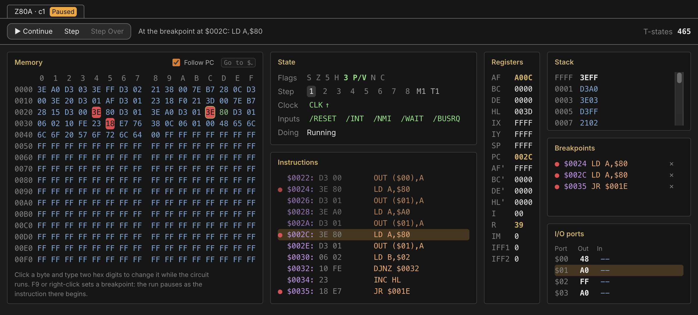
Right-click a CPU on the desk and choose Open CPU Monitor to watch it run. The monitor is a separate window that shows one CPU at a time, laid out like the Chip Designer's debugger. Each CPU on the desktop has a tab across the top; click one to switch to it. The tab shown carries a Running or Paused badge. While the window is open, selecting a CPU on the desk switches the monitor to it too. Nothing is shown until you press Run, apart from the breakpoint list. When you Stop, the monitor keeps the run's last moment on screen, dimmed.
Under the tabs is the debugger bar: Pause/Continue, Step and
Step Over (below), and a line saying where the CPU is paused, such as
At $8021: BEQ $8039, or At the breakpoint at $8021 when it stopped at one.
The window shows:
- Memory: 256 bytes. The opcode being run is highlighted, and the byte the
current bus cycle is reading or writing is outlined. The monitor reads each
address the way the CPU would: it asks your circuit's own decode logic which
memory chip answers there. An address that no memory chip answers shows
--, as do I/O chips such as a W65C22 (reading one of their registers could change it) and addresses where two chips answer at once. - State: the flags register, the step (which bus cycle of the instruction
is running; on a Z80, the M-cycle and its T-state), the clock phase, and the
CPU's input pins (reset, interrupts,
RDY/BEor/WAIT//BUSRQ). An asserted pin is drawn bold. - Instructions: eleven decoded lines. The middle line is the instruction in flight. The five lines above it are the instructions that actually ran, recorded as they happened. The five below are decoded ahead from memory in order, without following branches.
- Registers: one register to a line. If the run is paused partway through an instruction, they show how far it has got: PC has moved past the bytes already fetched, and a register being loaded changes once its byte is in.
- Stack: the top of the stack, one entry to a line, the newest first and
in bold: bytes on the 6502 (from S+1 to the end of page 1), words on the Z80
(from SP up). Click an entry to show its address in the memory block. Reset
leaves a 65C02's S at
$FD, so two entries are listed even before anything has been pushed. - Breakpoints: every breakpoint on this CPU, wherever it is, with the instruction there (below).
- I/O ports (Z80 only): the last byte each port was given by an
OUTand gave anIN, with the most recent port highlighted. An I/O port has no memory to read back, so what crossed it is all there is to show. The 6502 has no I/O space: its peripherals sit at ordinary addresses. - Cycles (6502) or T-states (Z80): how many clock cycles have run since Run.
The window is as large as it gets, so Stack and Breakpoints share the right column's height evenly and scroll when they are full.
The monitor makes the most sense at a slow clock, or with the clock paused and stepped by hand. At full speed it is a blur.
Moving around memory
The memory block follows the program counter, with PC's row in the middle,
until you look somewhere else. Clicking a byte, scrolling the block with the
mouse wheel, moving the selection off its top or bottom with the arrow keys
(or Page Up/Page Down), or typing an address into Go to ($8000,
0x8000 and 8000 all work) and pressing Enter pins the block there. Tick
Follow PC to have it follow the program again.
Changing memory
While the circuit runs or is paused, click a byte in the memory block and type
two hex digits to replace it. The cursor then moves to the next byte, so you
can type a run of values one after another. Enter writes a single digit (4
becomes $04), Escape drops it, and the arrow keys move the selection. A byte
can only be typed over while it is in the block on screen.
The new byte is written exactly where the CPU would read it, in whichever memory chip answers that address.
What happens to a byte you change in a ROM depends on the Keep ROM edits after Stop box. The box appears in the monitor's header as soon as you change a byte in a ROM during a run, and goes away again at Stop:
- Unticked (the default): the change lasts until you press Stop.
- Ticked: every ROM you changed during the run is saved when you press Stop, exactly as the memory inspector's Save would save it. A message names each chip that was saved. Like any change, it is an unsaved change to your project, and ⌘Z undoes it.
The box is read when you press Stop, so you can tick it at any point during the run. RAM is never kept, ticked or not: it forgets everything at Stop.
Changing registers
While the run is paused at the start of an instruction (where a breakpoint, a
Step or a Step Over leaves it), click a register and type its hex
digits; its last digit writes it, and Enter writes fewer. Escape lets it go,
and the up and down arrows move to the next register. Click a flag to flip it.
The 6502's B flag and its unused bit are not kept by the P register, so they
cannot be flipped.
A new PC moves the instruction fetch with it: the CPU carries on from the new address, and the instruction it was about to run at the old one is dropped from the record. If the run is paused partway through an instruction, the registers can only be read; press Step first.
What changed
While the run is paused, the registers and flag bits that changed since it last paused are highlighted. After a Step, that is what the one instruction changed; after Continue to a breakpoint, it is everything that changed on the way there. Changes you make yourself are not highlighted, and Stop starts over.
Breakpoints
To set a breakpoint, use any of these:
- Select a byte and press F9.
- Right-click a byte and choose Breakpoint.
- Click in the left margin of an instruction line.
A byte with a breakpoint turns red, and any instruction line at that address shows a red dot. The Breakpoints panel lists them all, so you can see the ones out of view too: click an address there to show it in memory, or × to remove it. The list is there before you press Run, so you can manage breakpoints before the program starts.
When the CPU reaches the instruction at a breakpoint, the run pauses right as the instruction begins: its opcode fetch is under way, and none of it has run yet. The monitor window comes forward on that CPU. From there you can step (below), or press Continue (F8) to run on until a breakpoint is reached again.
Pausing and stepping
The bar's first button is Pause while the circuit runs and Continue while it is paused; F8 presses it either way. They are the same as the main window's Pause and Resume.
While the run is paused (at a breakpoint, or by Pause), the monitor's Step button, or F6, runs the circuit on until the CPU starts its next instruction, and pauses there again. If an interrupt or a reset is taken instead, the step stops at the start of that sequence. A step also stops at any breakpoint it reaches, on any CPU. The whole circuit runs while it steps: every free-running clock and timed part moves on with the CPU, exactly as the main Step button moves them.
Step Over (F7) is offered when the instruction in flight calls a
subroutine: a 6502 JSR, or a Z80 CALL, CALL cc or RST. It runs the
whole subroutine and pauses at the instruction after the call, once the stack
is back where the call found it (so a recursive call returning to the same
place does not stop it early). A subroutine that reads data placed right after
the call and returns past it stops where it returns to. A breakpoint inside the
subroutine stops it
there. A short call is run at once, like a step. A long one, such as a delay
loop, carries on as a normal run at the circuit's own speed, and pauses when
the call returns; press Pause to give up on it where it is. The return
needs somewhere to keep its address: on a computer with no RAM behind the
stack, the subroutine never comes back to the call.
A step needs a free-running clock or a timed part to move the circuit. On a manual clock, click the clock instead. If the CPU starts nothing new within a few thousand clock edges (it is waiting for an interrupt, say), the step gives up and leaves the circuit paused where it got to.
F6, F7 and F8 work only while the monitor window has the focus. If the Chip Designer's debugger is also paused, they act on whichever of the two windows you are in. In the main window the function keys do nothing. While the debugger is holding the circuit in the middle of a clock edge, the monitor's Step does nothing: let the debugger finish first (Continue or To Settled).
Breakpoints fire even while the monitor window is closed. They are saved in the project, with the desktop they were set on: they last through Stop and Run, come back when you switch back to that desktop, and are there the next time you open the project. Setting or clearing one is a change to the project like renaming a desktop, so it marks the project unsaved, but it is not an edit to the circuit: it can be done while the circuit runs, and Undo does not take it back. A duplicated desktop keeps its CPUs' breakpoints; an exported one does not carry them.
Memory chips
The Memory group carries the address-indexed parts: a couple of generic teaching ROM/SRAM chips plus real-shaped EEPROM/EPROM/SRAM parts on wider DIP packages. Reads and writes are wired up the same way as every other chip in the catalog, but a non-volatile chip's contents live in a real file on disk and are programmed through a dedicated in-app tool rather than by the circuit itself. See Memory Chips & the Inspector for the full story — file-backing, the external programmer, and the hex/ASCII inspector.
The pin-assignments window
Right-click any chip — or a package-footprint discrete like the bar8iso
LED bar, which seats and rotates exactly like a DIP chip even though it isn't
one — and choose Pin Assignment, at the top of its context menu, to open
its pin-assignments window: a small, floating window separate from the
main desk, showing the physical DIP layout with the notch
at the top, pin 1 at the top-left, and pin numbers wrapping down the left side
and back up the right to the highest pin at the top-right, exactly as printed
on the part.
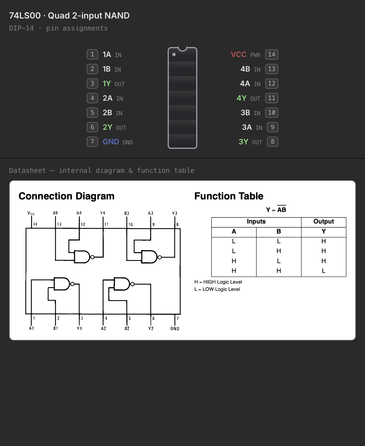
For a real chip this layout is always the canonical, fixed arrangement —
it matches the physical part regardless of how you've flipped it on the desk,
because a real chip's pin-1 dot is a physical feature of the package, not
something rotation changes. bar8iso is the one exception: it has no real
notch to key off, so its pin-assignments window reflects its current R
flip on the desk — rotate it and the corners in the dialog swap to match.
Below the pin map, chips that have one show the manufacturer's datasheet crop — a cropped image of the connection diagram or function table pulled straight from the source datasheet PDF. If a chip has no crop on file, that part of the window simply isn't there — the pin map alone is still complete and accurate.
When Settings → Data Sheets points at a local folder containing that chip's full datasheet PDF, the window also grows a small document button in its top-right corner; clicking it opens the PDF itself in your system's PDF viewer. This is independent of the built-in datasheet crop — you may have one, both, or neither for any given chip.
Example circuits
A pin map tells you where the pins are; it doesn't show you the part working. So almost every 74LS and CD4000 chip in the catalog ships with a worked example — a small bench built around that one part — and the pin-assignments window is where you reach it. Look for the circuit button in the window's top-right corner, beside the datasheet one.
Click it and the example arrives as a new desktop in the open project,
called 74LS138 example (or whichever part it is), already framed on screen.
Every one is the same bench, so once you can read one you can read them all:
- a 5 V brick feeding both power rails, and a clock for the clocked parts;
- switched inputs on the left, each throwing between +5 V and a pull-down so an input is never left floating — a part with more inputs than will fit gets a DIP switch bank over a resistor network instead. A CD4000 bench also ties every input it does not switch, spare gates included;
- the chip under test in the middle, straddling the trench;
- LED read-outs on the right, one per output, through its own resistor. An active-LOW output has its LED wired the other way up, so a lit lamp always means this output is asserted;
- a caption above the bench saying what the demo shows.
Press Run (Space) and flip the switches. Each example opens in a state chosen to show the part doing something.
The bench parts have examples of their own, each drawn as you would build it and captioned with what to try — most of them best run with Spice Lite on:
| Part | Desktops |
|---|---|
LM358 |
Comparator (a pot against half the supply, an LED on the output) · Amplifier (gain 2) |
ULN2003A |
Relay driver — one channel a relay, another an LED |
4N35, PC817 |
Isolated switch — a 5 V switch driving a 12 V LED on its own supply |
LM7805 |
9 V to 5 V (a 74LS04 on the regulated rail) · Under load (an electronic load drawing 300 mA) |
LM317 |
3.3 V — set by 240 Ω and 390 Ω |
| Relay | Transistor driver (with its flyback diode) · No flyback diode |
| Electronic load | Supply limit — a 500 mA supply under 250 mA, raise it and watch it droop |
| Speaker | Tone (a 555 at about 460 Hz) · Pitch (on a pot) · Key (a button on RESET) · Siren (one 555 moving the other's CONT) |
The two CPUs can't be shown by flipping switches either, so each example
is a whole computer, wired and ready: the CPU, an AT28C256 ROM with the
program already in it, a W65C22 VIA as the interface chip, a 16×2 LCD
on the VIA's ports, and a reset button. Press Run and the program sets the
LCD up and types Hello World a letter about every half second. Hold the
reset button and let go to watch it again; open the
CPU monitor to follow the program as it goes.
W65C02 example— the ROM fills$8000–$FFFFand the VIA sits in the low half, split by one 74LS04 onA15. The clock runs at 100 Hz.Z80A example— the ROM is all of memory, from$0000(the upper half repeats it), and needs no glue logic:/MREQis its chip enable and/RDits output enable. The VIA sits in the Z80's I/O space, selected by/IORQand written withOUT (n),A. The clock runs at 250 Hz, because a Z80 instruction takes more clock cycles than a 6502's. To build it for real, use the CMOS Z84C00: an NMOS Z80A cannot be clocked that slowly.
The ROM's program comes with the example, so you don't load anything. Like every ROM, the copy gets its own backing file, and the program is saved in your project with the rest of it.
The 555 is the exception: there is nothing to switch, because what it does
depends on how it is wired. Its example brings three desktops, one per
mode — NE555 Monostable example, NE555 Bistable example and
NE555 Astable example — each built the way you would on a bench, with an LED
on the output. Press the button on the monostable for a 1.1-second pulse;
press SET and RESET on the bistable to latch the LED on and off; the astable
blinks on its own at about 0.6 Hz. You land on the first; the others are the
next tabs along.
A few practical notes:
- It's an ordinary desktop and an ordinary unsaved change — it doesn't reach your project's file until you save, and you can rename it, edit it, or delete it like any other.
- Asking for the same example twice doesn't make a second copy; you land back on the desktop you already have. For the 555, only a desktop you have deleted is added again.
- Adding it stops a running simulation, exactly as switching desktops does.
- Parts with no bench have no button: the memory chips and the 65xx peripherals (a RAM can't be demonstrated by flipping switches at it — you can see them working in the CPUs' examples), the CD4000 RC timers (CD4047B, CD4098B, CD4528B, CD4538B and CD4541B — a timer's bench is its resistor and capacitor, not switches), the LM7809, LM7812 and LM7815 (the LM7805's example shows them all), and every other discrete, brick and wire. The CD4060B's example counts a clock brick on φI rather than running its oscillator.
Datasheets
The datasheet crops shown in the pin-assignments window are committed image
assets cut by hand from the manufacturer PDFs, not fetched or rendered at
runtime — they work offline and load instantly. A part with no crop on file
simply shows its pin map with no image below it: four 74LS parts have no
matching 74LS* datasheet (74LS164, 74LS193, 74LS27, 74LS76), and the
CD4000 parts' crops are still being cut. Pointing Settings → Data Sheets at your own folder of
manufacturer PDFs is a separate, optional feature — it doesn't add or replace
the built-in crops, it just adds the "open datasheet PDF" button for any part
whose PDF you have on hand.
Need a part the library doesn't have? Custom Chips covers designing your own.
See also Chips & Components for how chips seat into a breadboard, and Memory Chips & the Inspector for the memory group's file-backing and inspector.